Research Area I: Enabling Technologies
The research work in Research Area I “Enabling Technologies” aims to provide the technological base for fabrication of nanophotonic and teratronic components.
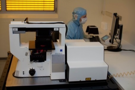
RA I provides the technological base for fabrication of nanophotonic and teratronic components. This involves process development, structural characterization and realization of demonstrator systems. One of the main challenges is to develop processes which allow patterning structures with nanometer resolution and high reproducibility. Research in RA I aims at advancing lithographic technologies like electron-beam lithography, direct-write two-photon lithography, and X-ray lithography as well as dry etching methods, nano-imprint technologies and thin-film deposition.
Moreover, processes for polymer waveguide fabrication and photonic coupling structures are in the focus of RA I activities. With regard to industrial exploitation of teratronics, methods for up-scaling of laboratory processes to small-scale production are envisaged, e.g., in the field of direct-write two-photon lithography.
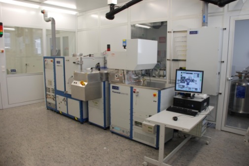
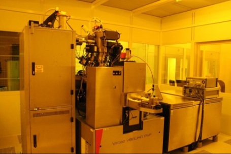
Activities in RA I are characterized by a strong interdisciplinary cooperation – it is the vivid exchange between technology-related activities, methodologies and applications that allows successful fabrication and functional demonstration of novel devices and structures. RA I can rely on cutting-edge cleanroom facilities and nanofabrication tools at the Institute of Microstructure Technology (IMT), the Institute of Nanotechnology (INT), and the Institute of Micro- und Nanoelectronic Systems (IMS). Moreover, RA I collaborates intensively with the Center for Functional Nanostructures (CFN) and with the Karlsruhe NanoMicro Facility (KNMF), an open-access high-tech platform that offers state-of-the-art micro- and nanotechnologies to users from industry and academia. This allows leveraging synergies in processing and characterization of functional nanostructures and devices.
Participating Institutes and Research Groups
 |
Institute of Microstructure Technology |
 |
Institute of Applied Physics
|
 |
Institute of Micro- and Nanoelectronic Systems |
.png) |
Chair of Dependable Nano Computing |
 |
Institute of Applied Physics and Institute of Nanotechnology |