Research Area III: Integrated Nanophotonics and Plasmonics
RA III aims at exploring novel photonic and plasmonic device concepts, fabricating them using both internal cleanroom facilities and cooperations with external technology platforms.
RA III explores novel photonic and plasmonic device concepts, exploiting the benefits of large-scale photonic integration. Teratronics relies on an intimate interplay of photonics and electronics, and future teratronic systems require scalable photonic device concepts that can be integrated in large numbers and that enable high-speed signal processing at lowest possible power consumption.
Within RA III, silicon photonics is one of the most important integration platforms. Silicon photonics enables large-scale foundry-based processing of photonic devices, and might even allow co-integration with electronic circuitry. Silicon as an optical material, however, falls short of properties that are indispensable for high-performance devices. These deficiencies can be overcome by the concept of silicon-organic hybrid (SOH) integration, which combines silicon-on-insulator (SOI) waveguides with dedicated organic cladding materials that provide the desired optical functionality. Our work on silicon photonics and SOH integration is complemented by plasmonic devices, which are particularly well suited for signal processing at THz bandwidths.
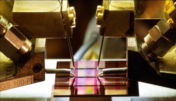
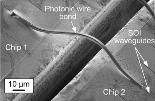
Moreover, we are working on novel hybrid system concepts that enable heterogeneous integration of photonic chips based on different material systems such as InP and SOI. These concepts of photonic multi-chip integration are based on the technique of photonic wire bonding, which we have introduced as a particularly versatile approach to connect nanophotonic circuits across chip boundaries.
In addition, we are investigating chip-scale frequency comb sources. These devices, e.g. rely on so-called Kerr frequency comb generation, where Kerr nonlinearities in a high-Q microcavity are exploited to transform a strong continuous-wave pump into a broadband spectrum of equidistant low phase-noise comb lines. We are in particular interested in exploiting the potential of Kerr comb sources for terabit/s data transmission and optical arbitrary waveform generation.
RA III builds upon fabrication technologies provided by RA I and by external partners such as the European technology platforms ePIXfab or Jeppix . For characterization and testing of devices, RA III can rely on a series of laboratories that are equipped with latest instrumentation. These laboratories are, e.g., run by the Institute of Photonics and Quantum Electronics (IPQ), the Institute of Microstructure Technology (IMT), the Institute of Nanotechnology (INT) or the Light Technology Institute (LTI).
Participating Institutes and Research Groups
 |
Institute of Photonics and Quantum Electronics (IPQ)
|
 |
Institute of Photonics and Quantum Electronics (IPQ) Institute of Microstructure Technology (IMT)
|
 |
Light Technology Institute (LTI) Institute of Microstructure Technology (IMT)
|
 |
Institute of Microstructure Technology (IMT)
|
 |
Institute of Micro- and Nanoelectronic Systems (IMS)
|
 |
Physical Institute (PHI)
|
 |
Institute for Data Processing and Electronics (IPE)
|
 |
Institute of Applied Physics and Institute of Nanotechnology
|
| ETH Zurich | |
 |
Institute of Electromagnetic Fields (IEF), ETH Zurich
|